Introduction
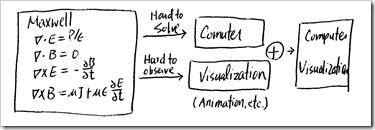
Maxwell published his famous equations governing all electrical and electronic phenomenon (with some quantum mechanics in some cases) in 1873. There are two problems. First, it is hard to solve these partial differential equations. Secondly, it is hard to grasp the physical picture of different EM phenomenon
幸運的是在某些條件下,我們可以簡化 Maxwell Equation 解決上述難題 。Fig. 2 分類可作的簡化。
(A0) only statics: div E = e, curl E = 0; div B = 0, curl B = J No interaction between E and B.
(A) Lumped circuit: 當系統的大小遠小於工作的波長,i.e. ( S << l = 1/f or f << 1/S)。系統的波動特性可忽略。可視為有一個固定的參考面電壓。以Maxwell equation 來說 :
curl E – k – 1/S >> dB/dt – f ==> curl E = 0 ==> define global voltage reference to ground: KVL
curl B = u J KCL
基本上這是電路學的理論基礎。也是最簡化的 Maxwell Equation。
Example: discrete circuit with low frequency
VLSI at very high frequency (s is small)
(B) Transmission line: 這時系統的大小相當或大於於工作的波長。意即波的特性不可忽略。但可就Maxwell equation 簡化。假設可以找到一連串參考面,定義局部的 curl E = 0 (no B field) and curl B = 0 (no E field and net J =0). 仍可定義出局部的電壓和電流,避開 E and B field calculation。TEM wave over transmission line 為例子。
Example:
電力線 60Hz over 100 km.
CAT5 ethernet cable.
Tools:
Smith chart for narrow-band system (電力線 microwave)
ABCD matrix for broad-band DSL
(C) Only wave : ignore J and e. still difficult!
(C1) 再來就必須面對 wave, 但若能簡化為 scaler wave equation 仍比 vector Maxwell equation 容易。
Maxwell equation –> Helmholtz wave equation (A) –> separation of variables –> scaler wave equation.
Example: geometric optics, gaussain beam optics (paraxial symmetry Helmholtz equation)
Tools: Gaussian
(D) if J and e cannot be ignore, and plus wave. This is the most difficult case
Example: CED, plasma physics
Lumped circuit model provides a simple approximation of a dipole antenna, it is useful but only valid within limited frequency range. The situation is shown in Fig. 6.
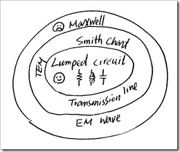
Fig. 6: Different abstraction in electrical discipline
Luckily, there is a another tool originally derived from transmission line, namely Smith Chart, provides useful physical insight and enough accuracy for understanding the dipole antenna. A brief introduction of Smith Chart is on the other article. Lumped circuit is a subset included in Smith Chart. Smith Chart (transmission line) is based on a specific EM wave called TEM (transverse EM) wave where the dynamic electrical and magnetic fields are perpendicular to the wave propagation direction. The majority of EM wave and waveguide either belong to the TEM domain or can be approximated by TEM wave. That is, Smith Chart is a very useful tool to solve most electrical problems.
The Smith Chart is plotted on the complex reflection coefficient plane in two dimensions and is scaled in normalized impedance (the most common), normalized admittance or both. Normalized scaling allows the Smith Chart to be used for problems involving any characteristic impedance or system impedance, although by far the most commonly used is 50 Ohm. With relatively simple graphical construction it is straightforward to convert between normalized impedance and the corresponding complex voltage reflection coefficient. Please refer wiki's Smart Chart for details and this reference.
How Smith Chart Work?
The keys are complex reflection coefficient, G, and normalized impedance, z, are plotted on the same chart as shown in Figure 1.
- The red x-y aisles represents the real and imaginary part of G. The intersecting point is the origin of the Smith Chart. Because |G| <= 1, the Smith Chart is fit inside a unit circle. The Smith Chart is not suitable for active circuit where the reflection coefficient might be larger than 1.
- The green circles represent zr = constant (zr is the real part of normalized impedance). The constant must be positive. The largest circle corresponds to zr=0 and also |G|=1. As zr increases to infinity, the circle converges to a point G=1 that is a open load.
- The black circles represents zi = constant (zi the imaginary part of normalized impedance). The constant can be positive/inductive, circles on the upper plane; or negative/capacitive, circles on the lower plane. The largest circle, x-axis, corresponds to zi=0. As zi increases to both positive/negative infinity, the circles also converges to a point G=1 that is a open load.
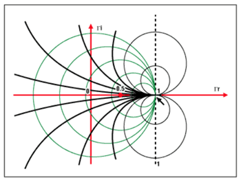
Fig. 1: Smith Chart Fundamental
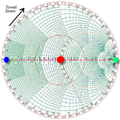
Fig. 2: Smith Chart
- The red-dot in Fig. 2 corresponds to no reflection (50Ohm load, G=0) ; the blue-dot corresponds to short load (G=-1); the green-dot corresponds to open load (G=1). The open load and short load is mirrored to each other through l/4 transformation as discussed in the next section.
Example:
Assume the characteristic impedance is 50Ω :
Z1 = 100 + j50Ω Z2 = 75 - j100Ω Z3 = j200Ω
Z4 = 150Ω Z5 = ∞ (open) Z6 = 0 (short)
Z7 = 50Ω Z8 = 184 - j900Ω
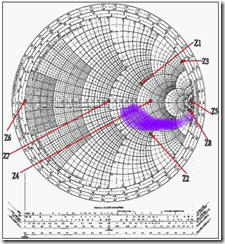
Fig. 3: Some Example Impedance
Note that a dipole antenna is close to open (Z5) at DC and becomes capacitive at lower frequency (Z8). If it is well matched at operating frequency, the impedance is close to 50Ohm (Z7); that is: Z5->Z8->Z2->Z7. Practically, the trajectory may be similar to the purple area because of non-perfect matching.
Transmission Line on Smith Chart
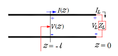
Fig. 4: Input Impedance with Transmission Line
One key advantage of Smith Chart is to obtain the input impedance of a load with transmission line shown in the above figure.
- For a lossless transmission line, the input impedance toward source is simply a clockwise rotation of the load impedance on the Smith Chart shown in Fig. 2. To remember clockwise rotation is to observe open load (green-dot) turns to capacitive (negative) load first; or short load (blue-dot) turns to inductive (positive) load first.
- One full circle rotation on Smith Chart represents half-wavelength (l/2) transmission line length; half circle rotation represents l/4 line length. Remember the famous quarter wavelength impedance transformation. From open to short is half circle rotation, corresponds to l/4 transmission line length. For any load after the l/4 transformation, the input impedance becomes the mirror point (with origin) on the Smith Chart.
Even though the Smith Chart is developed for system with transmission line, it is also very useful in lumped circuit for matching and analysis purpose in RF IC design shown in next sections.
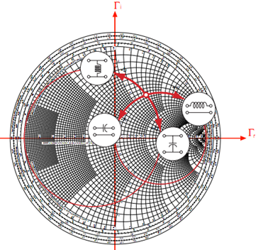
Admittance Smith Chart
The Smith chart is built by considering impedance (resistor and reactance). Once the Smith chart is built, it can be used to analyze these parameters in both the series and parallel worlds. Adding elements in a series is straightforward. New elements can be added and their effects determined by simply moving along the circle to their respective values. However, summing elements in parallel is another matter. This requires considering additional parameters. Often it is easier to work with parallel elements in the admittance world.
It turns out that the expression for y is the opposite, in sign, of z, and Γ(y) = -Γ(z). If we know z, we can invert the signs of Γ and find a mirror point situated in the opposite direction. Thus, an admittance Smith chart can be obtained by rotating the whole impedance Smith chart by 180°. This is extremely convenient, as it eliminates the necessity of building another chart. The intersecting point of all the circles (constant conductance and constant susceptances) is at the point (-1, 0) automatically. With that plot, adding elements in parallel also becomes easier. Math details can refer to this.
Lumped Elements on Smith Chart
When solving problems where elements in series and in parallel are mixed together, we can use the same Smith chart and rotate it around any point where conversions from z to y or y to z exist.
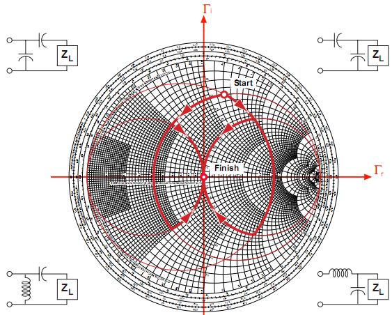
Let's consider the network of Fig. 5 (the elements are normalized with Z0 = 50Ω). The series reactance (x) is positive for inductance and negative for capacitance. The susceptance (b) is positive for capacitance and negative for inductance.
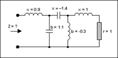
Fig. 5: Input Impedance of Lumped Elements
The circuit needs to be simplified (see Fig. 6). Starting at the right side, where there is a resistor and an inductor with a value of 1, we plot a series point where the r circle = 1 and the l circle = 1. This becomes point A. As the next element is an element in shunt (parallel), we switch to the admittance Smith chart (by rotating the whole plane 180°). To do this, however, we need to convert the previous point into admittance. This becomes A'. We then rotate the plane by 180°. We are now in the admittance mode. The shunt element can be added by going along the conductance circle by a distance corresponding to 0.3. This must be done in a counterclockwise direction (negative value) and gives point B. Fig. 7 shows the complete impedance transformation using Smith Chart.
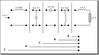
Fig. 6: Break the Network for Analysis
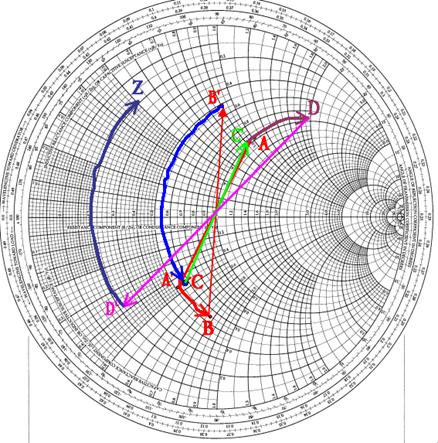
Fig. 7: Impedance Using Smith Chart
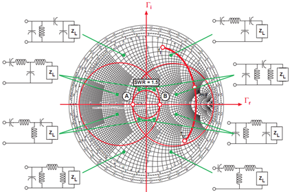
In summary
1. Add a serial L:
Move up (clockwise) along r=constant circle (circles intersects at (1,0))
2. Add a shunt L:
Move up (counter-clock) along g=constant circle (circles intersects at (-1,0))
3. Add a serial C:
Move down (counterclockwise) along r=constant circle (circles intersects at (1,0))
4. Add a shunt C:
Move down (clockwise) along g=constant circle (circles intersects at (-1,0))
The following figure shows the summary.
How to do matching using Smith Chart
L-match (8 types)
The following figure shows 4 different type of L match for positive reactance matching
Similarly, there are 4 types for negative reactance just exchange L and C.
pi/T-match
There are above 8 types of pi/T matching. Similarly, the mirror from positive to negative is to change L and C.
Examples
(I) Impedance Transformation from Tom Lee's RF CMOS book.
* If ZL is a pure resistance and ZL > Zo; only type2 (shunt-C with serial-L, or shunt-L with serial C) can convert Zin < ZL and Zin = ZL / ?? (only at resonant frequency, normally is a LPF or HPF)
* If ZL is a pure resistance and ZL < Zo; only type 4 (serial-C with shunt-L, or serial C with shunt C) can convert Zin > ZL and Zin = ?? (only at resonant frequency, normally is a HPF)
The above two L matches are in Tom Lee's book.
(II)
For dipole antenna below resonating frequency, it is like a serial RLC resonator; the resistor is higher than 50Ohm (air is 270Ohm); typical may be 75Ohm. The resonating frequency is assumed to be higher than the desired frequency. (Example, the LC frequency maybe 1GHz, but the operating frequency is 600MHz, etc.)
Therefore, the impedance is 75+X j Ohm (X is -200 to -50 Ohm). Is it possible to design a matching network?
Before/after resonating frequency
Condition 1: Re > 50Ohm and Im < 0 (capacitive load with high real impedance): example: dipole antenna before resonator
Condition 2: Re < 50Ohm and Im > 0 (inductive load and low real impedance): example: loop antenna
Condition 3: Re > 50Ohm and Im > 0 (inductive load with high real impedance??): example: dipole antenna after the resonator?
Condition 4: Re < 50Ohm and Im < 0 (capacitive load with low real impedance??): example: loop antenna
The matching choice (a) serial inductor; (b) parallel inductor. Both reduce the reactive part. The problem of (a) is real part is not change. Therefore choose (b) to reduce R from 72 to 50. Then use a serial capacitor to bring to the right matching point!!!
The best way to do is to use the center frequency first, not considering the entire frequency range. E.g. 400M to 800M, maybe use 600M for the matching purpose!!
Examine the L and Pi match
Impedance Matching with Smart Chart
http://www.maxim-ic.com/appnotes.cfm/an_pk/742/
- Match for maximum power transfer or optimize the noise figure or highest gain? Highest gain is always lowest noise figure?
- Maximum power transfer => Rs = RL*
- ?Ensure quality factor impact or access stability analysis because the matching network can be LPF or HPF or BPF.
- ? Can we replace RLC with scattering wave analysis using smith chart for both passive and active component (cmos?) there is no concept of impedance at low frequency? wrong, can I still normalize to 50Ohm since there is still finite value of impedance?


